Introduction
I proposed a follow-up from the previous discussion on the STM32F103, where I suggested picking up a TTL-to-USB adapter which I could use to implement a more concrete, performant communication channel between the MCU and host:
Ideally, I hope to write my own driver for the USB-TTL adapter, so that I can gain experience in dealing with peripheral state.
So, I purchased some CP2102 break-out boards, and let them collect dust for a little while as I mentally prepared myself for the pain that would inevitably be having to work with it. CP2102 is a USB-to-UART bridge, which has readily available COM drivers for us to interface on Windows, so it seemed the most intuitive choice.
As expected, it involved a couple days of pain and regret before I surpassed my first goal: getting the first real "Hello, embedded world!" displayed on my computer concocted entirely by the MCU. The discussion that follows covers some of the tricky portions that I encountered, and some of the important bases to cover when working with peripherals.
The first step: connecting it up physically. Correctly.
Much like the ST-Link debugging interface that I'd been using to semi-host the STM32F103 (i.e. enable debugging capabilities and I/O between my PC and the MCU,) the CP2102 break-out contains silkscreen which (most likely) will correspond to pins on your MCU development board.
Those pins being GND, 3V3 (or 5V), and then TXD and RXD. More than likely your MCU will not have dedicated nor pre-configured UART transmission/receival pins, but certain pins will be configurable to be used as such through STM32 registers.
On my board, the A2/A3 pins (as annotated on the silkscreen) correspond to PA2/PA3, which you may deduce either from your manufacturer's datasheet, or the place from which you ordered the MCU from will likely have a graphic depicting which break-out pins correspond to which GPIO pins.
Note that Pxy refers to port x, pin y--useful nomenclature which will be referred to in the reference manual.
Now, searching PA2 in the datasheet (which contains the pinout information) tells us that it may be configured for the following functions:
TIM2_CH3, TIM5_CH3, TIM9_CH1, I2S2_CKIN, USART2_TX, EVENTOUT
Principally important is USART2_TX, therefore it will be our UART transmission pin, by the same method we can discover that PA3 is for receival.
I spent a lot of time debugging, validating, and verifying code that may well have been working, just to find out that connecting the CP2102's TXD to the pin responsible for UART TX is in fact not correct. It's not constructed as a pass-through, but rather TXD means transmission from the host to the MCU, so it will need to be received into our allotted RX pin (PA3 in my case.)
Once the four pins (assuming you're connecting only 3V3 or 5V, and not both for whatever reason) are connected, and it shows a red light once connected, you're off to the races.
Some key differences between the STM32F103 and STM32F411
Aside the key differences in flash, SRAM, and increased clock frequency, there's some other differences that posed as subtle obstacles in trying to port my STM32F103 hardware abstraction layer (HAL) over:
- The STM32F4x series of MCUs are Cortex-M4, unlike the former which is Cortex-M3. The quintessential difference is just that the Cortex-M4 has a floating-point unit coprocessor (FPU) (which lets us do more math :),) which may have adjusted offsets for CPU-specific registers and regions. Consult the ARM documentation, I didn't have any issues in my time, but I had no need to use anything non-STM32-specific.
- The boundary addresses are almost all entirely different: I ran my code several times with the wrong RCC (clock-related) register boundary address, and it was entirely silent outside of the consequence it didn't work. Always double-check your addresses.
- Some register structures are modified. This, again, will likely show no obvious symptoms, so foremost due diligence is important.
It's always confusing to navigate reference manuals with hundreds of pages, block/timing diagrams, and seeing concepts that seem related to your goals, but are entirely unrelated in the bigger picture. Always aim to get a minimal working proof of concept that you understand conceptually, and worry about the particulars of efficiency and correctness later. It's sometimes much easier to understand why something's poorly done than to figure out why something doesn't work at all.
Where should we start with the code?
So, this was naturally the trickiest part, since delving into peripherals with an entirely theoretical understanding means that you may be prone to overthinking, over-researching, or just generally confusing yourself. It's unsurprisingly very complex at first sight--so many clocks, bridges (low and high performance, for either hardware and peripherals), hundreds of registers with names which are beyond obnoxious, and much more.
Clocks
The first crucial thing to understand is clocks, since they're intimately coupled with serial baud-rate (just how fast data is transmitted/received.) All they do fundamentally is generate "pulses" at constant-time intervals, which we interpret as frequency: a 10Hz clock generates 10 pulses every second, so we could schedule a task on each pulse--fairly simple.
As most simple things we have in life, they are inextricably powerful building components for systems which need to have a heartbeat, or rhythm, by which they perform all their functions. For you and I to have a conversation, we need to understand when the other is talking, as to not talk over one another. The same principle follows for serial transmission.
At the highest level in the STM32, we have the system clock, which is just a generalisation of whichever specific clock "implementation" we have available or chosen. This primary clock drives everything we care about, and it lends itself to the derived clocks that power buses. So called derived since they may have a lesser or larger frequency proportional to the system clock.
Buses
Then we continue to buses, highways for data between components, whether internal to the CPU or across peripherals, like UART for our CP2102 interface. The implementation of these is specific to Cortex-M4 and the AMBA-3 specification, but simply put, there are three high-performance buses (AHBs) and one peripheral bus (APB.)
Pedantically speaking, although steering more towards a comprehensive theoretical understanding, there are instruction/data/system/DMA "buses" which are all arbitrated by the bus matrix, although the ARM manual coins these instead as interfaces which, then, subsequently uses one of the AHBs to communicate.
For the the STM32 specifically, it seems like there's only one AHB and two APB buses, which I won't question despite it being contraindicative to the ARM manual, but at least it's simpler. Oh, and the AHB is split into two AHB1 and AHB2 with different characteristics for both, presumably for optimisation.
Now, the CP2102 will be communicating across one of these peripheral buses, which we'll have to choose between since why would they be qualitatively identical? Our life would be too easy if that were so.
Connecting clocks, buses, and peripherals
I naively thought that we would just have a fixed frequency from which we could tune our baud-rate from the get-go, and connecting everything together will be like a jigsaw. No, these MCUs are designed for very powerful flexibility in power optimisation (hence their ubiquity in industrial applications,) and as far as the system is concerned from a reset state, everything is pretty much turned off except for the system clock. We'll have to turn everything on that we need to move forward.
So, clocks drive buses which drive peripherals: which clocks do we need to enable for what we want to achieve? A rule of thumb seems to be that anything that involves registers will likely have an associated clock, this meaning that the GPIO pins and the UART mechanism will have clocks, since, well, we need to specify how we want to interpret the data coming into the pins, and likewise for UART transmission.
That's about it. It's all just clocks, timing, zzz.
Sounds boring, what about the actual code?
Okay, so let me jot down what we need to do functionally to get what we need working:
- Mandatory STM32 setup, initialisation vector setup, copying
.dataover to SRAM, etc. - Enable the clocks for the things we want to use
- Configure our GPIO pins for reading and writing
- Enable the UART functionality on those pins
- Configure the UART functionality to match whatever we're using on the receiving side
- Send a nice message over to ourselves
- Pop a bottle of champagne
The first step is covered by simply importing over the boilerplate code we've written for the STM32F103 and adjusting certain register boundary addresses according to the STM32F411 and Cortex-M4 manual. Then, we need to enable the clock for the appropriate GPIO pins, which in the case of UART would be across port A.
Enabling the clocks
Referencing the manual, we deduce from Table 1: register boundary addresses that the GPIO peripherals are driven by the AHB1 bus, so we may likely configure the functionality through some RCC_AHB1xx sub-register. Let's take a look:
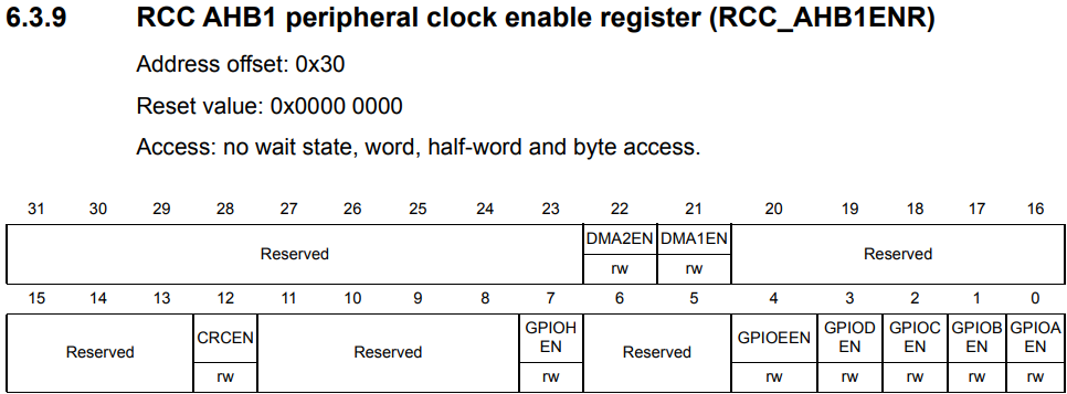
Lo and behold, GPIOAEN (GPIO port A ENable) is what we're looking for to enable the peripheral clock since it's designated as Set and cleared by software, so all we need to do is:
REG_RCC->AHB1ENR |= 0b1 << 0;
And it's done! Now what about UART? The same Table 1 tells us USART2 is designated to APB1, and USART1 is APB2: so which should we pick? The datasheet holds all the answers in a monolithic block diagram:
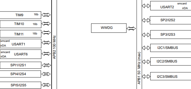
APB1 clocks up to 50MHz, whereas APB2 may go to 100MHz. So, the question is do we really care? The answer for embedded applications that couldn't be less mission critical is no. Let's choose APB1 since it's probably more economical on power usage with a lower clock-frequency.
So, we need to enable USART2EN inside RCC_APB1ENR, following the same pattern as before:
REG_RCC->APB1ENR |= 0b1 << 17;
Now, we don't like magic numbers, so these should be extracted into macros like RCC_AHB1ENR_GPIOAEN and RCC_APB1ENR_USART2EN, and perhaps even further as macros like RCC_APB1_ENABLE(clock) for readability.
Note that the documentation refers to USART, whose difference to UART seems to just be synchroneity through two additional pins XCK and XDIR, removing the need for specifying transmission rate with an agreed upon baud-rate. We don't use this functionality, so we can simply refer to what we're doing as UART.
Configuring the pins for GPIO and UART
So, the only thing we need to configure for GPIO is to specify to the MCU its intention is UART, which is an alternate function (AF), and its speed. The manual indicates we need to adjust the MODER (port MODE Register) and set pins 2/3 to 0b10, indicating both pins will have alternate functions assigned to them.
I have it extracted into a tidy macro to refrain from the reader needing to see bit-shifting vomit, but hopefully this is not your biggest concern:
GPIOx_MODER_CONFIGURE(REG_GPIOA, 2, GPIO_MODER__AF);
GPIOx_MODER_CONFIGURE(REG_GPIOA, 3, GPIO_MODER__AF);
Now before we assign which alternate functions, we should likely set the speed to make sure the electrical characteristics are stable (it seems like a sound reason;) naturally, OSPEEDR controls this parameter, and is set similarly in code:
GPIOx_OSPEEDR_CONFIGURE(REG_GPIOA, 2, GPIO_OSPEEDR__FAST);
GPIOx_OSPEEDR_CONFIGURE(REG_GPIOA, 3, GPIO_OSPEEDR__FAST);
Note that there's lots of GPIO ports, hence GPIOx, and likely lots of other things that are grouped, so don't waste time making hundreds of macro definitions when you could just pass the specific thing as the first parameter. My macro definition for GPIOx_OSPEEDR_CONFIGURE looks like this:
#define GPIOx_OSPEEDR_CONFIGURE(reg_gpio, y, val) \
  ({ \
    (reg_gpio)->ospeedr &= ~(0b11 << (2 * (y))); \
    (reg_gpio)->ospeedr |= (val) << (2 * (y)); \
  })
Not particularly pretty, handsome, or efficient, and it could certainly be made more compiler-agnostic, but it maintains a level of decent macro practice.
Does the speed really matter?
The datasheet is unsurprisingly more cryptic when it comes to understanding what frequency this means the pins can run at, since it's far more intertwined with electrical engineering--but, here's what seems relevant:
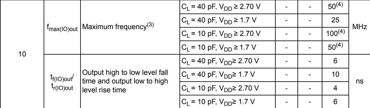
GPIO_OSPEEDR__FAST is Ob10 which corresponds with the lefthand-side column, as for what the capacitive load and $V_{DD}$ refers to... I don't really know. We can likely assume $V_{DD} \geq 2.70 V$ since we're powering on 3.3V, and since we're on APB1 we can likely infer that 50MHz will be the maximum frequency we can get anyways, so the capacitive load doesn't matter.
I tried looking in more depth, but it's fairly complicated, and all these characteristics seem to determine is how quickly the signals transition from low-to-high levels, so higher speed is a quicker transition and lower speed is more slewed--which might be important if we were doing anything significant.
Assigning the pins to do UART
So, we want to assign an alternate function to the two pins, fortunately we have a GPIO AFR (Alternate Function Register) which does this exactly:
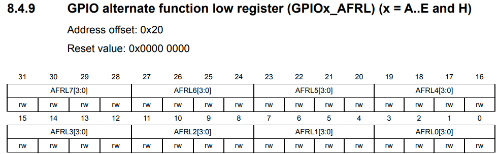
The AFR is split into low/high since each pin uses 4 bits but we have 16 ports, thus needing 64 bits. We can abstract this away with macro magic since they may be inconsequentially regarded as the same. Now, which alternate function specifier do we want?
Figure 17 somewhere above, but in the same GPIO section, will give us the answer:
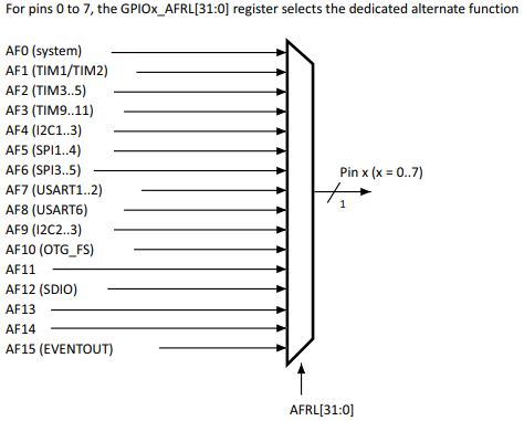
AF7 enables both UART1 and UART2 for the pins we designate, so there is our answer: we set each AFR pin to 0b0111. The macro I wrote looks like this:
#define GPIOx_AFR_CONFIGURE(reg_gpio, y, val) \
  ({ \
    stm_word_t adj_y = (y > 7)? y - 8: y; \
    if (y > 7) \
      (reg_gpio)->afrh = \
        ((reg_gpio)->afrh & ~(0b1111 << (4 * adj_y))) | (val << (4 * adj_y)); \
    else \
      (reg_gpio)->afrl = \
        ((reg_gpio)->afrl & ~(0b1111 << (4 * adj_y))) | (val << (4 * adj_y)); \
  })
We just clear the existing bits at the position, and bitwise OR it against our new val, ensuring we choose the right register based on which pin we wish to address.
Configuring UART so our computer understands us when we talk
Now all the sudden this becomes a little more complicated since we need to know what actual clock-frequency we're running at to calculate the baud-rate. This means we need to know the derived clock frequency of the APB1 bus, since that's what UART2 is running from.
Math jump-scare!
As a forenote, the formula we're working with is:
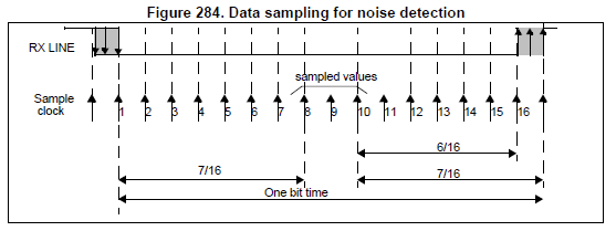
$f_{CK}$ refers to the APB1 clock frequency, and $\text{Baud}$ is our desired baud. $\text{OVER8}$ is 1 if we're using oversampling by 8, otherwise 0 if we're oversampling by 16; this is a parameter which seems to result in better noise detection by sampling the receiving line at higher intervals as shown below:
Typically, we'll be using oversampling by 16, so our formula reduces to:
$\text{USARTDIV}$ is the value we will be putting into our baud-rate register, which will be touched upon soon.
How do we figure out the clock frequencies?
I'll try to run through this section quickly since it's not really interesting. In theory we can source our system clock-frequency from many sources, but typically at reset we'll be using the HSI internal clock, which according to the datasheet demonstrates a typical frequency of 16MHz.
RCC_CFGR (ConFiGuration Register) has a two-bit bitfield SWS which is--
--set and cleared by hardware to indicate which clock source is used as the system clock
Great, so it can be either HSI, HSE or PLL. Frankly, if it's either of the other two, then it's up to you to figure it out since it's likely external or something you've configured yourself. Either way, we can systematically figure out which, and so by verifying it's HSI we know we're at 16MHz.
Now, the same configuration register also contains values named prescalers which downscale the main clock frequency by a constant divisor: the AHB clock is prescaled from the system clock, and the APB clocks are prescaled from the AHB clock. These values are available from the HPRE and PPRE1/2 bits.
  stm_word_t ahb_div = (RCC_CFGR_HPRE < 8)? 1 : (2 << (RCC_CFGR_HPRE - 8));
  stm_word_t apb1_div = (RCC_CFGR_PPRE1 < 4)? 1 : (2 << (RCC_CFGR_PPRE1 - 4));
  stm_word_t ahb_clk = clk_freq / ahb_div,
             apb1_clk = ahb_clk / apb1_div;

  iprintf (
    "AHB clock: %lu MHz\nAPB1 clock: %lu MHZ\n",
    ahb_clk / 1000000,
    apb1_clk / 1000000
  );
clk_freq is determined in a switch-statement earlier based on the SWS bits.
Now how do we calculate the baud-rate?
Well, first we need to take a look at the UART register map:
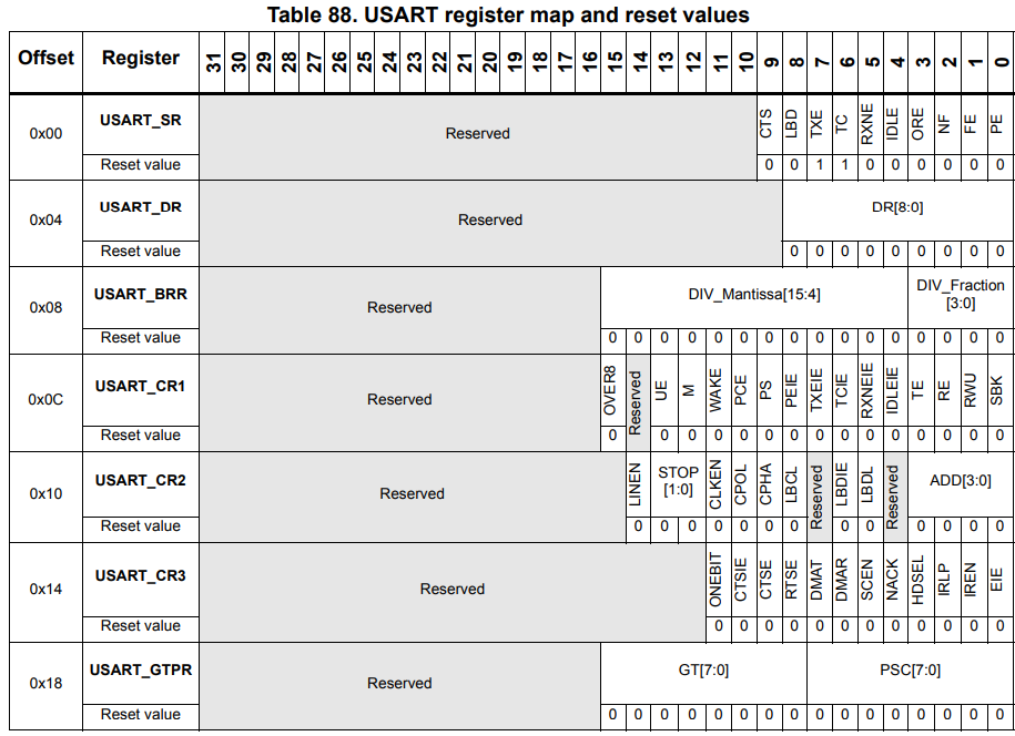
USART_BRR is the register we're interested in at the moment. The term mantissa might bring back horrors from having to deal with floating points, but thankfully it's not too egregious here:
So, DIV_Fraction is just the decimal portion of the division from the other $\text{USARTDIV}$ formula, but multiplied by 16. As a small example, if our $\text{USARTDIV} = 25.125$, then $\text{DIV_Mantissa} = 25$ and $\text{DIV_Fraction} = 16 * 0.125 = 2$. Nothing complicated, just stuff those into the 12/4 bits and forget about it.
uint32_t
calculate_usart_brr (uint32_t apb_clock, uint32_t baud_rate)
{
    uint32_t usartdiv_16x = (apb_clock + (baud_rate / 2)) / baud_rate;
    uint32_t mantissa = usartdiv_16x / 16;
    uint32_t fraction = usartdiv_16x % 16;
    uint32_t brr = (mantissa << 4) | (fraction & 0xF);
    return brr;

}
The usartdiv_16x calculation is just essentially:
So we're just rounding to the nearest integer instead of truncating, just for that little bit of additional precision, and then we pack it into the mantissa and fraction bits. That's all we have to do.
Are we ready to turn it on?
Not quite yet, not if we don't tell UART we're ready to receive and transmit. These are toggled by the UE (USART Enable), RE (Receiver Enable) and TE (Transmitter Enable) bits in CR1 referenced in the previous diagram:
REG_USART2->cr1 = USART_CR1_UE | USART_CR1_TE | USART_CR1_RE;
Preferably ensure CR1 is cleared before you set BRR.
Now we're ready to do whatever we want! Everything's explained and there's no additional registers we'll need outside of what has already been mentioned, so here are the functions for reading and transmitting:
char
usart2_read (void)
{
    while (!(REG_USART2->sr & USART_SR_RXNE));
    return REG_USART2->dr;
}

void
usart2_putc (char c)
{
    while (!(REG_USART2->sr & USART_SR_TXE));
    REG_USART2->dr = c;
    while (!(REG_USART2->sr & USART_SR_TC));
}

void
usart2_puts (const char* const c)
{
  for (stm_word_t i = 0; c[i]; ++i)
    usart2_putc (c[i]);
}
Nothing ground-breaking, we make sure we have something to read, and conversely that the transmission buffer is empty before we write something else, and optionally wait until the transmission was marked as complete. Now the line that everything has built towards:
usart2_puts ("hello, embedded world :)\n");
Assuming you have the COM drivers and PuTTY connected at the corresponding baud-rate, you should get this:

Beautiful.