The reference quietly pad some certain register fields without explicitly stating there's a reserved area between them, leaving you to figure it out from the offsets. Good thing we're validating sizes otherwise that would have been obnoxious to figure out.
What's the difference between different general-purpose timer groups?
TIM2-5 + TIM23-24:
16/32 bit reload counters
- 16 bit only on tim3/4
- 32 bit on the rest
16 bit programmable prescaler
Synchronization circuit
4 independent channels
- input capture, output compare, PWM (edge/center-aligned), one pulse
trigger input for ext. clock
Supports incremental (quadrature) encoder and hall-sensor circuitry
interrupt generation for:
- update, trigger event, input capture, output compare
TIM12-14:
16 bit reload counter
16 bit programmable prescaler
Synchronization circuit (ONLY for tim12)
up to 2 independent channels (ONLY 1 for tim12)
- input capture, output compare, PWM (edge-aligned), one pulse
interrupt generation for:
- update, trigger event, input capture, output compare
NO trigger event for tim13-14
TIM15-17:
16 bit reload counter
16 bit programmable prescaler
Break input to put the timer’s output signals in the reset state or a known state
Complementary outputs with programmable dead-time
Repetition counter to update the timer registers only after a given number of cycles of the counter
Synchronization circuit (ONLY for tim15)
up to 2 independent channels (ONLY 1 for tim16-17)
- input capture, output compare, PWM (edge-aligned), one pulse
interrupt generation for:
- update, trigger event, input capture, output compare
NO trigger event for tim16-17
Basically TIM2-5 and TIM23-24 are the most versatile, and then TIM12-14 seem the simplest, and TIM15-17 have some special functionality that might be useful for niche applications.
Digital-analog converter (DAC)
DAC1_OUT1 on PA4, DAC1_OUT2 on PA5.
We're working with pulse-code modulated (PCM) media which is sampled at 22,050Hz and represented by unsigned little-endian 8-bit units. So, we're working with 8-bit right-aligned data which we must write to DAC_DHR8Rx, which is subsequently converted to the internal DHR register, and after $t_{settling}$, the output voltage is available on the appropriate chip pin.
The output voltage is determined between 0 and $\text{DACoutput}$, where: Where DOR is the data-output register, determined by the data-holding register (DHR.)
The DAC has two channels, though we only need 1. We need to set TSEL appropriately to sample at an appropriate frequency, i.e. from the timer which we are using to generate the 22kHz signal, as well as TEN and EN to enable triggers and the DAC channel itself.
The appropriate timer signal is dac_chx_trgy where y is packed into 4-bits in TSEL.
Double-buffering, circular buffers, integrating with the DAC
First we need to enable the appropriate clocks for TIM6, DAC1 and USART2.
Then enable AF7 on GPIOA so we can receive USART data on PA10.
To configure USART, we enable the receive-flag, and configure our baud-rate to at least 22kHz, but 57600 or 115200 are fairly standard baud-rates which will reduce latency/jitter.
Then, we need to configure DMA on the USART side. Provide a tunable parameter which determines the sample buffer-size, e.g. if we store 256 8-bit samples then we will have $256 / 22.05 = 11.61\text{ms}$ of audio data buffered from our USART transmitter.
Since we're double-buffering, by the time first half is ready to be processed--assuming a sufficient baud-rate--the second half will also be ready, and so a continuous stream will exist for the DAC to process.
1. Enable DMA.SxTRBUFF enabled since the manual says it's necessary for USART
2. Enable DMA.SxCR.CIRC on USART for circular buffering so that new data will overwrite from the beginning of the buffer: hopefully we've processed it!
3. Enable DMA.SxCR.DBM for double-buffering mode, DMA_SxM0AR and DMA_SxM1AR are the target buffers whose pointers are swapped on transmission complete (TC.)
4. Enable DMA.SxCR.HTIE (half-transmission) and DMA.SxCR.TCIE (TC) interrupts
- On half-transmission: we have data ready for the DAC! Set a flag so that on the next TIM6 cycle it knows that we're happy for it to consume the audio data in the first buffer
- On transmission completion: the second audio data buffer is ready, so it should be consumed as long as the first data buffer was also consumed. We should not underrun USART and attempt to receive more data while either indicator flags are still active.
Voltage scaling
PWR.D3CR.VOS configures the voltage scaling level for the system clock, though by that it means it enables the ability to clock beyond certain thresholds, but by itself doesn't affect anything. Variable system clock frequency scaling can be performed by using PLL as the clock source, scaling against another clock like HSE/HSI/CSI up or down based on tunable parameters.
Timer clock frequency
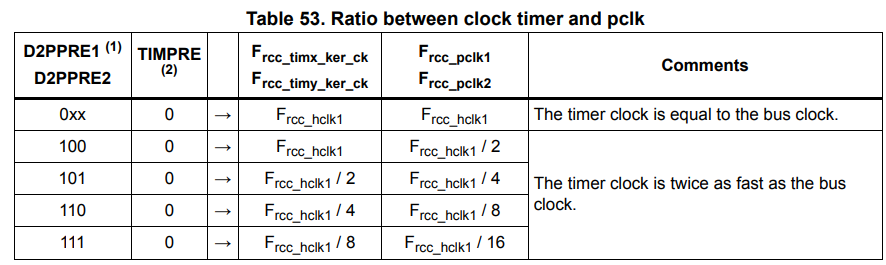
Odd quirk, if the AHB clock is divided by a factor of 2 or more, the timer clock runs at twice the AHB's frequency.
Regardless, if we want to generate a sample event at 22.05kHz, we need to "clock" when our overflow event occurs, which is determined by both the prescaler and autoreload value: Both denominator expressions added by 1 to avoid division-by-zero. So, considering we have $f_{\text{TIM6}}$ as: We need to optimise $\text{PSC}$ to improve clock granularity, and then refine it down to 22.05kHz with an appropriate $\text{ARR}$ value. Consider: If we let $\text{ARR} = \text{PSC}$, then we have: Which for a 4MHz clock, we calculate 12.47 (2 d.p.), although we deviate $\pm 8\%$ with rounding error, which is fairly substantial.